


| LCD Type | a-Si TFT/RGB-stripe/ADS | ||
| Viewing Direction | All | ||
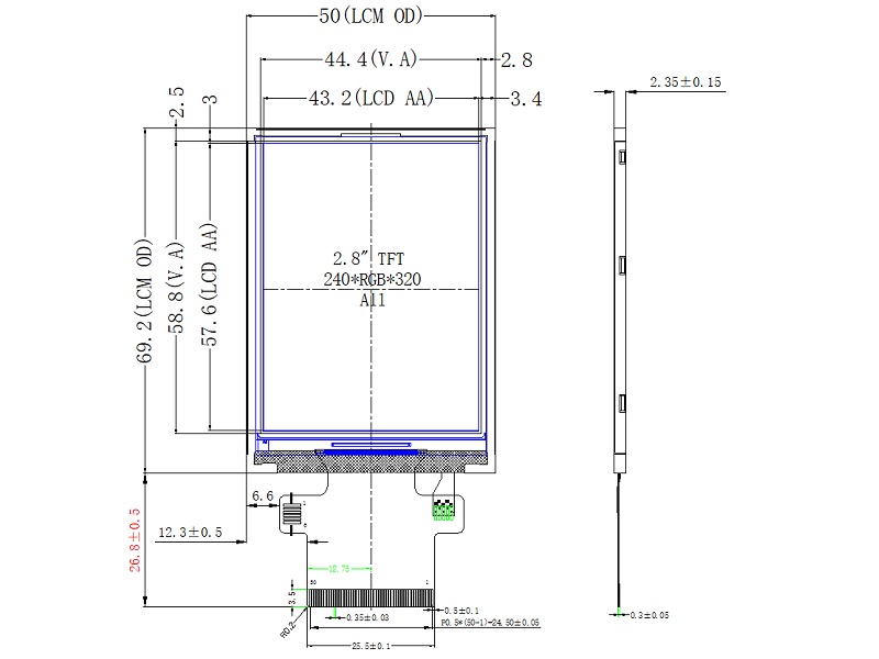
| Number of Dots | 240RGB(H)×320(V) | ||
| LCM Outline(H*V*T) | 50×69.2×2.35 | ||
| Active Area(H*V) | 43.2×57.6 | ||
| Operating Temperature | -20~+70℃ | ||
| Power Supply Voltage | VCC=2.8V/IOVCC=1.8V | ||
| BL Power Consumption | 240mW(4P) | ||
| Panel Power Consumption | 18mW | ||
| LCD Controller | JD9851 | ||
| LCD interface | MCU/RGB/SPI | ||
| LCM Brightness | 280cd/m2 | ||
| Contrast Ratio | 1200 | ||
|
Pin No. |
Symbol |
I/O |
Description |
|
1 |
LED_K |
P |
Backlight cathode |
|
2~5 |
LED_A |
P |
Backlight anode |
|
6~9 |
IM0~3 |
I |
The MCU interface mode select.
|
|
10 |
/RESET |
I |
Reset pin. Initializes the LCM when low. |
|
11 |
vs |
|
Vertical (Frame) synchronizing input signal for RGB interface If not used, please fix to the VDDI or DGND. |
|
12 |
hs |
|
Horizontal (Line) synchronizing input signal for RGB interface If not used, please fix to VDDI or DGND. |
|
13 |
dotclk |
|
Dot clock signal for RGB interface operation If not used, please fix this pin at VDDI or DGND. |
|
14 |
de |
|
Data enable signal for RGB interface operation If not used, please fix this pin at VDDI or DGND |
|
15~32 |
DB17~DB0 |
I |
DB[17:0] are used as MCU parallel interface data bus & RGB interface data bus. If not used, please fix this pin at VDDI or DGND |
|
33 |
SDO |
O |
SPI interface output pin. The data is output on the falling edge of the SCL signal. If not used, let this pin open |
|
34 |
SDI |
I |
When IM3: Low, SPI interface input/output pin. When IM3: High, SPI interface input pin. -The data is latched on the rising edge of the SCL signal. If not used, please fix this pin at VDDI or DGND level |
|
10 |
/RD |
I |
Read enable clock input pin |
|
9 |
/WR |
I |
Write enable clock input pin |
|
8 |
RS |
I |
Selects the register. Low : Index / status; High : Control |
|
7 |
/CS |
I |
Chip select pin. Active: low |
|
39 |
TE |
O |
Tearing effect output. If not used, please open this pin. |
|
40~41 |
IOVCC |
P |
Digital IO Pad power supply |
|
42 |
VCI |
P |
Analog power supply |
|
43 |
GND |
P |
Power ground |
|
44 |
CTP_SCK |
I |
I2C clock input |
|
45 |
CTP_SDA |
I |
I2C data input and output |
|
46 |
CTP_IRQ |
I |
Interrupt request to the host, or Wakeup request from the host. |
|
47 |
CTP_RES |
I |
External Reset, Low is active |
|
48~50 |
GND |
P |
Power ground |


 中文
中文 English
