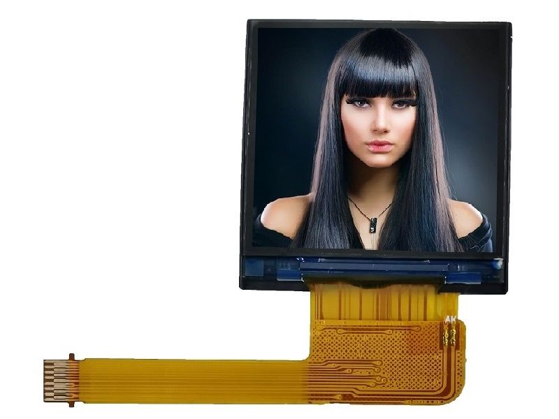


| LCD Type | 1.4"/a-Si TFT/RGB-stripe/ADS | ||
| Viewing Direction | all | ||
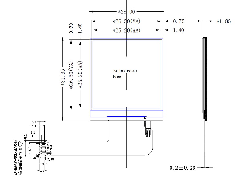
| Number of Dots | 240RGB(H)×240(V) | ||
| LCM Outline(H*V*T) | 28×31.35×1.8 | ||
| Active Area(H*V) | 25.2×25.2 | ||
| Operating Temperature | -20~+70℃ | ||
| Power Supply Voltage | VCC=2.8V | ||
| BL Power Consumption | 180mW(3p) | ||
| Panel Power Consumption | 13mW | ||
| LCD Controller | JD9851 | ||
| LCD interface | 4-line 8bit serial | ||
| LCM Brightness | 450cd/m2 | ||
| Contrast Ratio | 1200 | ||
|
Pin No. |
Symbol |
I/O |
Description |
Note |
|
1 |
SCL |
I |
serial clock |
|
|
2 |
GND |
P |
Power ground pin. |
|
|
3 |
RS |
I |
data/ command selection |
|
|
4 |
TE |
O |
Tearing effect output pin to synchronies MCU to frame rate, activated by S/W command. If not used, please open this pin. |
|
|
5 |
GND |
P |
Power ground pin. |
|
|
6 |
CS |
I |
Chip Selection Pin -Low Enable. |
|
|
7 |
RESET |
I |
This signal will reset the device and it must be applied to properly initialize the chip. Signal is active low |
|
|
8 |
SDA |
I/O |
serial data input/output |
|
|
9~10 |
GND |
P |
Power ground pin. |
|
|
11 |
VLED- |
P |
Backlight LED Cathode |
|
|
12 |
VLED+ |
P |
Backlight LED Anode |
|
|
13 |
VDDIO |
P |
Power1.8V Supply for I/O system. |
|
|
14~15 |
VDD |
P |
Power2.8V Supply for Analog, Digital System and Booster Circuit. |
|


 中文
中文 English