


| LCD Type | a-Si TFT/RGB-stripe/ADS | ||
| Viewing Direction | All | ||
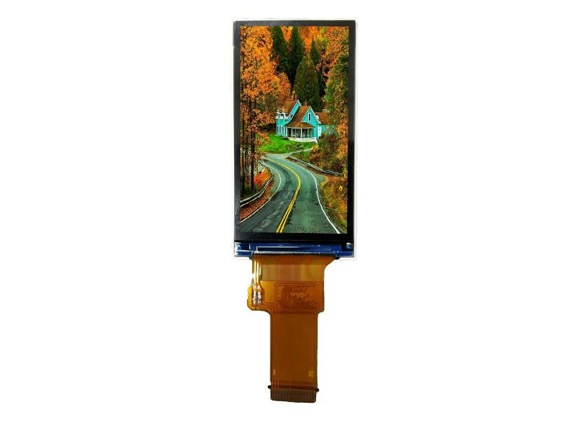
| Number of Dots | 320RGB(H)×480(V) | ||
| LCM Outline(H*V*T) | 53.19×74.33×2.0 | ||
| Active Area(H*V) | 51.27×68.36 | ||
| Operating Temperature | -10~+60℃ | ||
| Power Supply Voltage | VCC=2.8V | ||
| BL Power Consumption | 360mW(6P) | ||
| Panel Power Consumption | 25mW | ||
| LCD Controller | ST7789 | ||
| LCD interface | MIPI | ||
| LCM Brightness | 300cd/m2 | ||
| Contrast Ratio | 1200 | ||

|
Pin No. |
Symbol |
I/O |
Description |
|
1 |
LED_A |
P |
Backlight anode |
|
2~3 |
LED_K |
P |
Backlight cathode |
|
4 |
VCI |
P |
2.85V For Analog power supply |
|
5 |
IOVCC |
P |
1.85V Power supply for I/O system. IOVCC must be lower than or equal to VCI. |
|
6 |
/RESET |
I |
Reset pin. Initializes the LCM when low. |
|
7 |
TE |
O |
Tearing effect output. If not used, please open this pin. |
|
8 |
NC |
- |
NOT Connect |
|
9 |
GND |
P |
Power ground |
|
10 |
D0P |
I |
Positive polarity of low voltage differential data signal. |
|
11 |
D0N |
I |
Negative polarity of low voltage differential data signal. |
|
12 |
GND |
P |
Power ground |
|
13~14 |
NC |
- |
NOT Connect |
|
15 |
GND |
P |
Power ground |
|
16 |
CLKP |
I |
Positive polarity of low voltage differential clock signal |
|
17 |
CLKN |
I |
Negative polarity of low voltage differential clock signal |
|
18 |
GND |
P |
Power ground |
|
19~20 |
NC |
- |
NOT Connect |
|
21 |
GND |
P |
Power ground |
|
22~23 |
NC |
- |
NOT Connect |
|
24 |
GND |
P |
Power ground |
|
25 |
CTP_INT |
I |
Interrupt request to the host, or Wakeup request from the host. |
|
26 |
CTP_SDA |
I/O |
I2C data input and output |
|
27 |
CTP_SCL |
I |
I2C clock input |
|
28 |
CTP_RST |
I |
External Reset, Low is active |
|
29 |
CTP_VCI |
P |
3.3V power supply For CTP |
|
30 |
GND |
P |
Power ground |


 中文
中文 English